- 您现在的位置:买卖IC网 > Sheet目录996 > NCP1028LEDGEVB (ON Semiconductor)EVAL BOARD FOR NCP1028LEDG
�� �
�
�NCP1028�
�This� difference� might� not� be� seen� as� a� problem,� but� some�
�design� specifications� impose� stringent� conditions� on� the�
�maximum� output� current� capability,� regardless� the� line�
�input.� Hence� the� need� for� an� OPP� input� …�
�Since� we� want� to� limit� the� power� to� 12.8� W� at� high� line,�
�let� us� calculate� the� needed� peak� current:�
�10� k� W� and� R� OPPU� made� of� a� series� string� of� 4� 1.0� M� W�
�resistors� plus� a� 10-turn� 1.0� M� W� potentiometer� set� at� its�
�maximum� value.� An� amp-meter� is� inserted� in� series� with�
�pin� 7� and� a� volt-meter� monitors� its� voltage� with� respect� to�
�ground.� Once� the� power� supply� is� powered,� slowly� rotate�
�the� potentiometer� and� observe� both� voltage� and� current�
�From� equation� 6:� Ipeak� +�
�2Pout�
�FSWLp� h�
�=� 693� mA� to�
�going� up� at� pin� 7.� At� a� certain� time,� as� voltage� and� current�
�increase,� the� controller� will� shut� down� the� power� supply.�
�deliver� 12.8� W� at� high� line.�
�Compared� to� our� 735� mA,� we� need� to� decrease� the�
�setpoint� by� 6%� roughly� when� V� in� equals� 350� Vdc.�
�The� NCP1028� hosts� a� special� circuitry� looking� at� the�
�couple� voltage/current� present� on� pin� 7.� Figure� 36� shows�
�how� to� arrange� components� around� the� controller� to� obtain�
�Over� Power� Protection.�
�Bulk�
�The� current� at� this� time� is� the� one� we� are� looking� for.�
�Suppose� these� experiments� lead� to� 80� m� A� with� a� pin� 7�
�activation� voltage� of� 2.45� V.� Final� resistor� equations� are:�
�VbulkH� =� 375� Vdc� ;� the� maximum� voltage� at� which� OPP�
�must� shut� down� the� controller�
�V� bulkL� =� 200� Vdc� ;� the� minimum� voltage� below� which�
�OPP� is� not� activated�
�I� OPP� =� 80� m� A� ;� the� current� in� pin� 7�
�V� f� =� 2.45� V� ;� the� voltage� of� pin� 7� at� the� above�
�condition�
�ROPPU�
�ROPPL� +�
�VbulkH-VbulkL�
�IOPP(VbulkL-Vf)�
�Vf� +� 27� k� W�
�(eq.� 7)�
�ROPPH� +� ROPPL� bulkL�
�Current�
�Setpoint�
�Over� Power�
�Protection�
�OPP�
�V�
�Vf�
�-Vf�
�+� 2.2� M� W�
�(eq.� 8)�
�ROPPL�
�GND�
�Figure� 36.� A� resistive� network� reduces� the�
�power� capability� in� high-line� conditions.�
�First,� you� need� to� know� the� required� injected� current� and�
�the� voltage� across� pin� 7� to� start� activating� OPP.�
�Experiments� consist� in� wiring� Figure� 36� circuit� and�
�running� the� power� supply� in� conditions� where� it� must� shut�
�down� (e.g.� highest� input� voltage� and� maximum� output�
�current� per� specification).� For� this,� R� OPPL� can� be� put� to�
�V� DD�
�IRR�
�Ramp�
�If� the� OPP� feature� is� not� needed� for� some� designs,� it� is�
�possible� to� ground� it� via� a� copper� wire� to� the� adjacent�
�ground� pin.� This� can� help� to� develop� a� larger� copper� area�
�in� an� application� where� the� thermal� resistance� is� an�
�important� parameter.�
�Ramp� Compensation�
�When� operating� in� Continuous� Conduction� Mode�
�(CCM),� current-mode� power� supplies� can� exhibit�
�so-called� sub-harmonic� oscillations.� To� cure� this� problem,�
�the� designer� must� inject� ramp� compensation.� The� ramp� can�
�either� be� added� to� the� current� sense� information� or� directly�
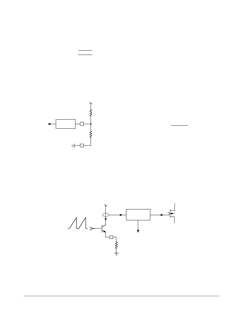
�subtracted� from� the� feedback� signal.� Figure� 37� details� the�
�internal� arrangement� of� the� ramp� compensation� circuitry.�
�Gate� Reset�
�Control�
�Vp�
�RR�
�Figure� 37.� The� Internal� Feedback� Chain� and� the� Ramp� Compensation� Network�
�http://onsemi.com�
�21�
�发布紧急采购,3分钟左右您将得到回复。
相关PDF资料
NCP1216AFORWGEVB
BOARD EVAL NCP1216A 35W
NCP1351LEDGEVB
EVAL BOARD FOR NCP1351LEDG
NCP3065BBGEVB
BOARD EVAL NCP3065 MR16 BOOST
NCP3066SCBCKGEVB
EVAL BOARD FOR NCP3066SCBCKG
NCP5005GEVB
EVAL BOARD FOR NCP5005G
NCP5006EVB
EVAL BOARD FOR NCP5006
NCP5030MTTXGEVB
EVAL BOARD FOR NCP5030MTTXG
NCP5602EVB
EVAL BOARD FOR NCP5602
相关代理商/技术参数
NCP1028P065G
功能描述:电流型 PWM 控制器 NCP1028 65 KHZ RoHS:否 制造商:Texas Instruments 开关频率:27 KHz 上升时间: 下降时间: 工作电源电压:6 V to 15 V 工作电源电流:1.5 mA 输出端数量:1 最大工作温度:+ 105 C 安装风格:SMD/SMT 封装 / 箱体:TSSOP-14
NCP1028P100G
功能描述:电流型 PWM 控制器 NCP1028 100 KHZ RoHS:否 制造商:Texas Instruments 开关频率:27 KHz 上升时间: 下降时间: 工作电源电压:6 V to 15 V 工作电源电流:1.5 mA 输出端数量:1 最大工作温度:+ 105 C 安装风格:SMD/SMT 封装 / 箱体:TSSOP-14
NCP1028PL065R2G
功能描述:交流/直流开关转换器 ANA 1 FREQ GULLWING RoHS:否 制造商:STMicroelectronics 输出电压:800 V 输入/电源电压(最大值):23.5 V 输入/电源电压(最小值):11.5 V 开关频率:115 kHz 电源电流:1.6 mA 工作温度范围:- 40 C to + 150 C 安装风格:SMD/SMT 封装 / 箱体:SSO-10 封装:Reel
NCP102MBGEVB
功能描述:电源管理IC开发工具 NCP102 4W MOTHERBRD EVB
RoHS:否 制造商:Maxim Integrated 产品:Evaluation Kits 类型:Battery Management 工具用于评估:MAX17710GB 输入电压: 输出电压:1.8 V
NCP102SNT1G
功能描述:低压差稳压器 - LDO LDO LINR REG CONTRL RoHS:否 制造商:Texas Instruments 最大输入电压:36 V 输出电压:1.4 V to 20.5 V 回动电压(最大值):307 mV 输出电流:1 A 负载调节:0.3 % 输出端数量: 输出类型:Fixed 最大工作温度:+ 125 C 安装风格:SMD/SMT 封装 / 箱体:VQFN-20
NCP1030
制造商:ONSEMI 制造商全称:ON Semiconductor 功能描述:Low Power PWM Controller with On-Chip Power Switch and Startup Circuits for 48V Telecom Systems
NCP1030_06
制造商:ONSEMI 制造商全称:ON Semiconductor 功能描述:Low Power PWM Controller with On−Chip Power Switch and Startup Circuits for 48V Telecom Systems
NCP10301
制造商:ONSEMI 制造商全称:ON Semiconductor 功能描述:AC-DC Offline Switching Controllers/Regulators